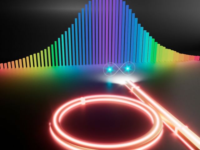
The QPL develops nonlinear integrated photonic, nanophotonic, and optoelectronic devices and systems for quantum computing, communications, networking, and sensing. We specialize in photonic device modeling, design, fabrication, and testing, heterogeneous integration of different materials and components, and photonics systems development and packaging. Current research thrusts include (1) nonlinear quantum photonics (III-V materials for entanglement, squeezing, and multi-photon quantum state engineering), (2) integrated photonic systems (heterogeneous III-V-on-SiN, quantum sensors, packaged entanglement chips and switches), and (3) cryogenic integrated photonic technologies (deterministic quantum sources, cluster-state generation, and cryo-modulators).
We thank the many sponsors of our current projects, including the DoD, DARPA, AFOSR, DOE, NNSS, NASA, NSF, Cisco, Google, and IEE. Our research is highly collaborative, including projects co-led with several groups around the world including Canada, Germany, France, Japan, Denmark, and Italy. Students in the group have many opportunities to participate in or lead these projects, including international travel to conferences, attending summer schools and workshops, and participating in research exchanges.


Resources & Facilities
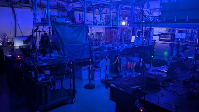
The Quantum Photonics Laboratory is located in Henley Hall -- the home of the Institute of Energy Efficiency (IEE) and the QPL. Our lab is equipped with state-of-the-art instrumentation and quantum photonic experiments and testbeds, with capabilities that include:
- Photonic Integrated Circuit (PIC) Testing: We have several PIC testing stations with fiber input/output, DC and RF electrical probes, microscopes for positioning and stabilization, a variety of tunable lasers in the NIR and telecommunications bands, and high-speed electronic control instrumentation.
- Cryogenics: A 4K closed-cycle cryostat with XYZ nanopositioning, low-working distance optical access, and DC-to-microwave electronic probe capabilities. The QPL also operates a 10 mK dilution refrigerator system with a customized vibration-stabilized optical confocal microscope combined with microwave electronics in the Quantum Foundry Low-Temperature Optics Lab in CNSI.
- Spectroscopy: The QPL houses a suite of quantum photonic device testing and benchmarking tools for characterizing nonlinear quantum photonic circuits, semiconductor nanophotonic structures, quantum emitters, and 2D materials. Additional capabilities include time-resolved micro-photoluminescence, resonance fluorescence with high-NA imaging, and rapid spatial scanning capabilities.
- Quantum Optics: We utilize superconducting nanowire single-photon detector arrays and time-correlated single-photon counting modules for photon correlation measurements with ~20 picosecond resolution across 8 channels. Experiments include second-order auto-correlation spectroscopy, Hong Ou Mandel interferometry, Franson interferometry, and quantum state tomography.
- Quantum Opto-Electronic Microscopy: We've developed a novel microwave-optical heterodyne spectroscopy probe for studying hybrid electro-opto-mechanical quantum systems at 10 mK.
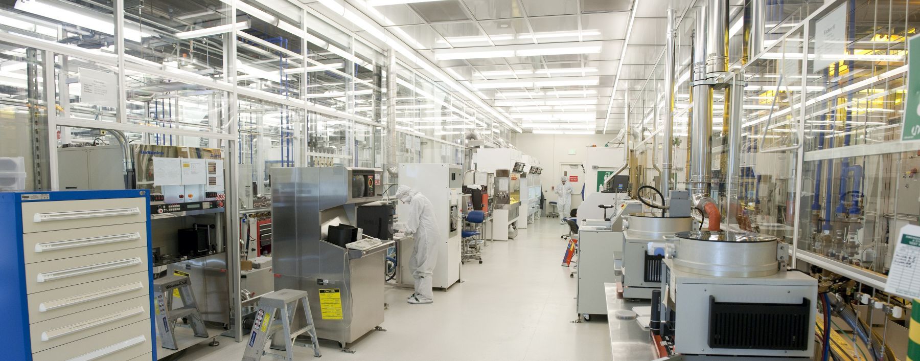
In addition to collaborating with several research groups and laboratories across campus, we also leverage the state-of-the-art facilities available at UCSB for material growth, device nanofabrication, and characterization, including the
Materials Research Laboratory (MRL)
UCSB Nanofabrication Facility (Nanotech)
California Nanosystems Institute (CNSI)
We design our devices using Lumerical and Comsol, design the PICs using open-source software, fabricate all of our devices in the UCSB nanofab, and characterize the devices in our labs before benchmarking and testing on campus or sending them to industry, academic, and government partners for collaborative R&D.